Although conventional and printed electronics have a lot in common and are based on similar principles, their manufacturing processes each pose their own challenges for the materials used. While copper has offered numerous advantages in conventionally manufactured electronics for many decades, the results in printing processes have so far been less convincing. The minimal copper particle size in the printing pastes inevitably leads to rapid oxidation and thus to extremely low conductivity. Although silver can circumvent these problems, it also costs considerably more - and hinders the further development of the industry.
Printed functional layers can now be soldered
The binder ITZ is currently conducting promising tests with copper pastes for electronics printing. Additional chemical components remove oxygen, prevent copper oxidation during the drying process and thus maintain the conductivity of the print results. The prototypes of the new generation of pastes already reduce the amount of material used by 30 percent, and the series could achieve savings of up to 90 percent.
This opens up completely new possibilities: Copper pastes can now also be used for pad printing and do not require complex etching or sintering processes. A silicone pad transfers the copper structures from the printing mould directly onto the component to be printed. The functionalised component then only needs to be thermally dried.
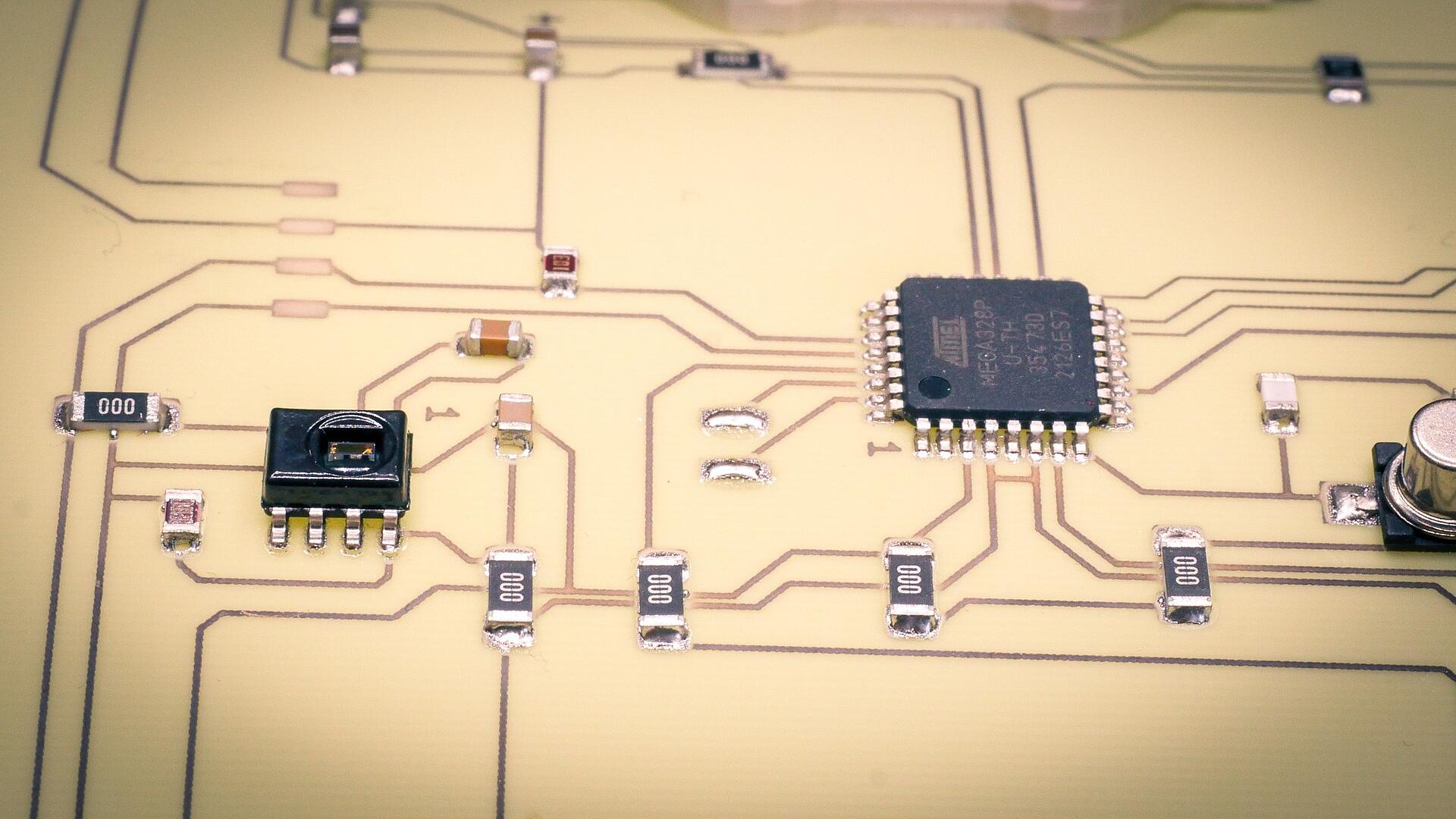
This results in functional layers that are significantly more resilient and can even be soldered on. Cables, stranded wires or connectors (e.g. LIF or ZIF) can be easily attached to printed contact points, and even the application of printed copper conductors on SMD components is no longer a challenge.
These results should significantly increase the acceptance of printed components once again. Above all, the new generation of pastes means that nothing stands in the way of the hybrid fusion of conventional and printed components.
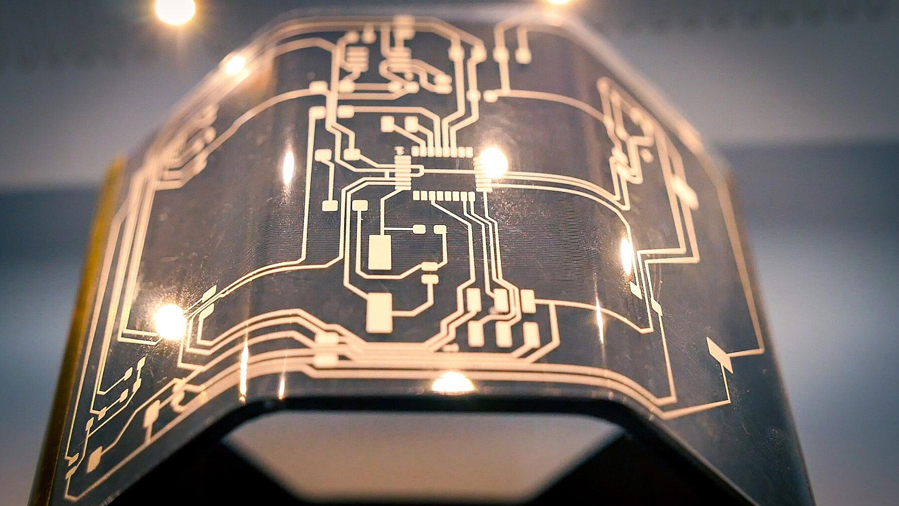
The best of two worlds
The mix of conventional and printed components offers enormous potential for savings and innovation. Printed elements are characterised by their low weight, high flexibility, low height and practically infinite design freedom. As sensors for force or temperature measurements, they are ideal for use with PCB-based measurement technology.
The price advantage of copper pastes is also increasingly paying off for single-use products, which are indispensable in healthcare or logistics, for example. Printed sensors, copper antennas and SMD NFC chips turn medicine packaging or efficacy test strips into smart and cost-effective sources of information that conveniently output and store data on storage temperature, type of active ingredient or time of administration via mobile phone.
The first results of the binder ITZ's innovative printing tests on the new generation of pastes were presented at this year's Technology Mountains Innovation Forum in Donaueschingen.