Printed electronics enable completely new applications with previously unimagined material properties. The binder process can be used to provide 3D surfaces with a wide variety of functions.
binder ITZ specialises in screen and pad printing. With these high-precision printing techniques, electronic functional layers such as conductor tracks or insulation layers can be applied directly to the desired component. This not only saves customers time-consuming intermediate steps such as foiling. Costs and weight are also reduced.
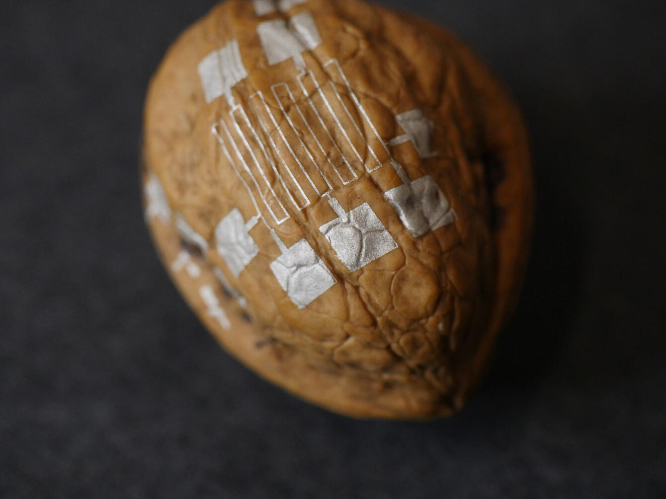
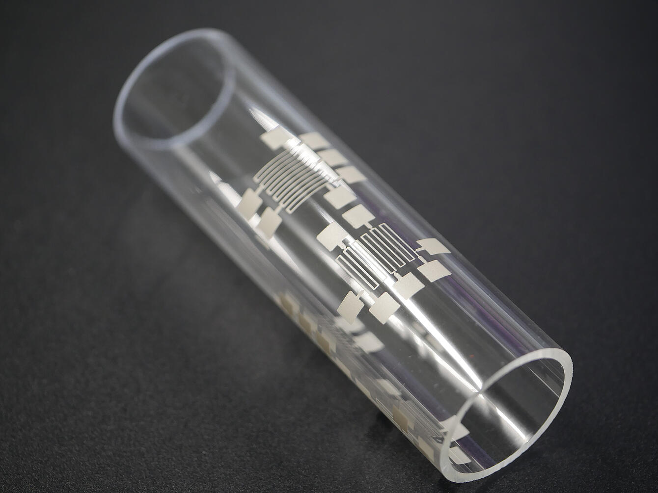
Complex geometries and surface structures are no longer a challenge in terms of functionality. Whether flexible circuit boards or transparent circuits: We take our customers' products to the next level and also set new standards in terms of design.